PCB Design Guide | Industrial PCB Design Guide
PCB Design Guide | Industrial PCB Design Guide
PCB (Printed Circuit Board) design is one of the most critical engineering processes that directly determines the performance, reliability and manufacturability of electronic systems.
When design is not done correctly, both production costs increase and field failure risk rises.In this guide, we systematically cover the basic principles of PCB design, DFM approach, footprint and connector selection criteria.
What Is PCB Design?PCB design is the engineering process that ensures electronic components are electrically correctly connected on a printed circuit and physically placed in a manufacturable way.
Main goals:Electrical accuracySignal Integrity (SI)Power Integrity (PI)Manufacturability (DFM - Design for Manufacturing)Thermal managementBasic Stages of PCB Design Process
1. Schematic Design: The stage where the electrical logic of the circuit is established. Circuit diagram & logic.
2. Component Placement: Physical placement of components on the board. Placement is critical according to signal flow.
3. Routing (Track Routing): Signal paths, power and ground lines are drawn. Controlled impedance control.
4. DFM Check: Design is verified in terms of manufacturability. Manufacturing check.
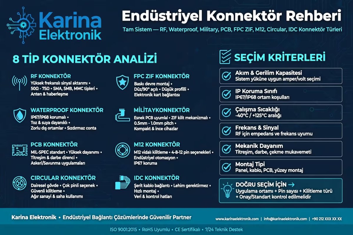
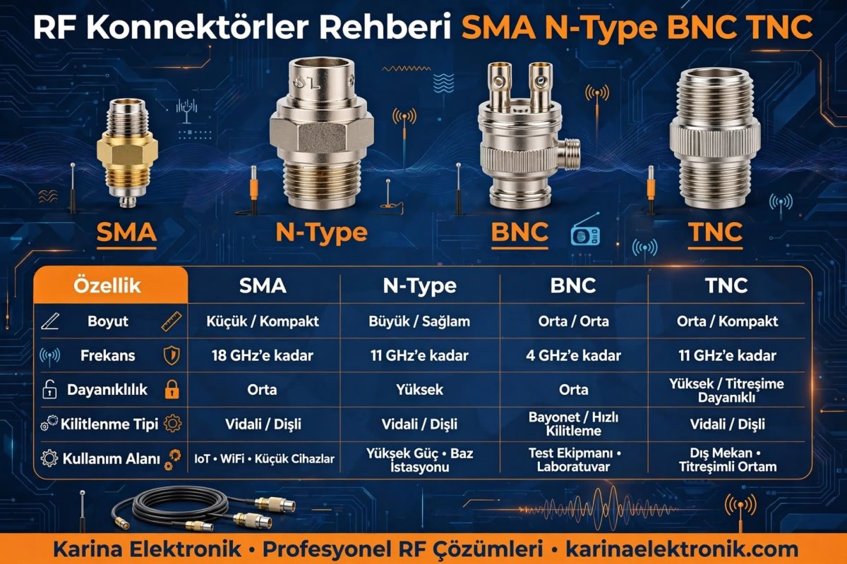
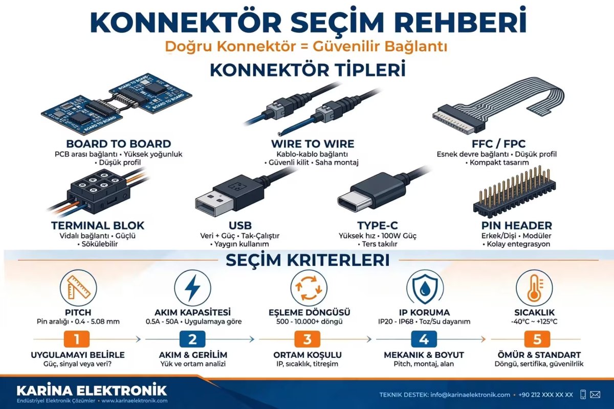
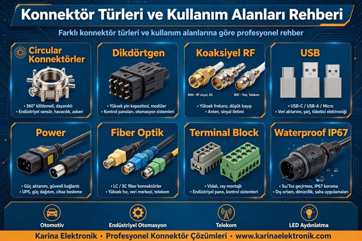
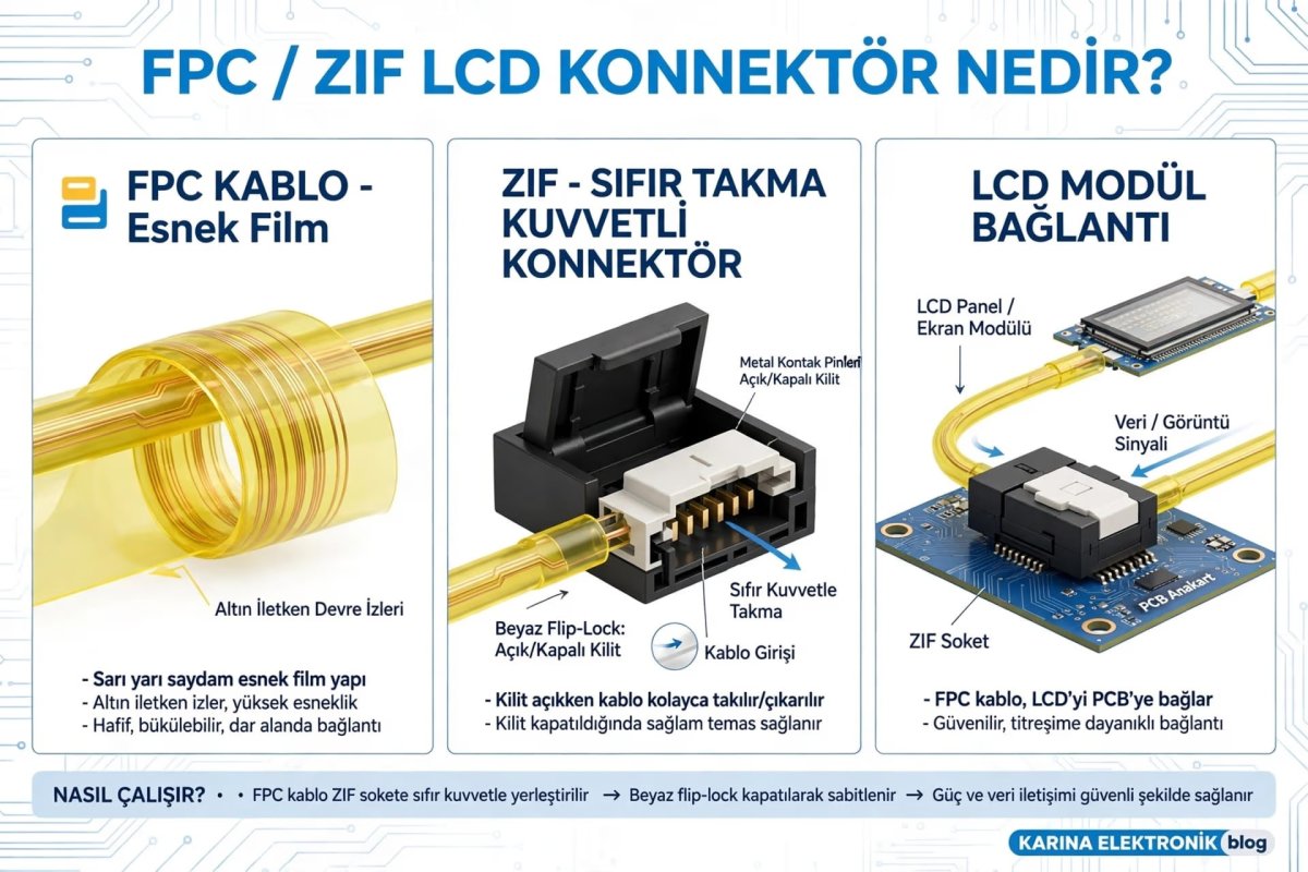
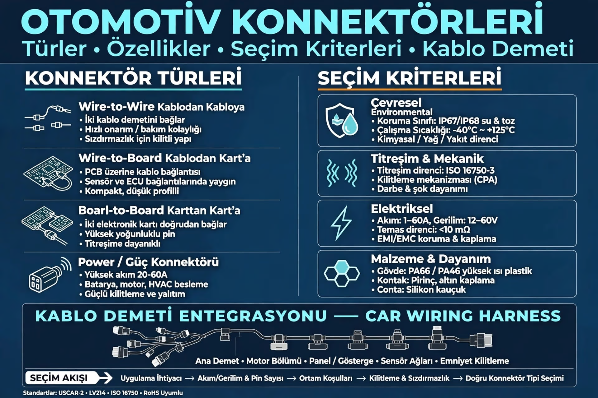
5. Gerber Output: Production files are prepared. Factory files & export.Footprint and Land Pattern DesignOne of the most critical points of PCB design is footprint (pad layout) design. Wrong footprint can cause:Cold solderTombstoningShort circuitAssembly errorsIPC-7351 Standard is the global reference at this point.What Is DFM (Design for Manufacturing)?DFM is designing the PCB so that it will not give errors during production.Basic DFM rules:Minimum trace width complianceVia-pad distance controlSolder mask clearanceReflow tolerancesMost Common Mistakes in PCB DesignWrong footprint usageInsufficient ground plane design (discontinuous ground)Lack of impedance control in high-speed linesWrong connector selectionNeglecting thermal gapsHow Does Connector Selection Affect PCB Design?Connector selection is not just a mechanical decision; it also affects signal integrity and product life.Wrong connector selection can lead to:Signal lossMechanical looseningEMI problemsProduction incompatibilityBest Practices in PCB DesignDo not neglect ground plane usage - uninterrupted groundKeep high-speed signals short - crosstalk minimizationOptimize via countMake component placement according to signal flowUse thermal relief - heat dissipationImportance of IPC Standards in PCB DesignIPC standards provide global quality standard in PCB manufacturing.IPC-7351: footprint / land pattern standardIPC-A-600: visual quality / acceptabilityIPC-2221: general design rulesConclusion
PCB design process is a balanced engineering discipline between electrical accuracy, mechanical durability and manufacturability. Correct design approach both reduces production costs and increases product reliability.
For detailed info: https://www.karinaelektronik.com/