PCB Design Errors and Critical Points - DFM Guide
PCB Design Errors and Critical Points - DFM Guide
Errors made in the PCB design process can lead to serious failures and performance losses in the production stage.Especially designs made without complying with DFM (Design for Manufacturing) principles cause soldering problems, connector incompatibilities, signal integrity problems and increased production costs.In this article, we examine the most common mistakes in PCB design and their effects on the production process.
7 Most Common Critical Mistakes in PCB DesignInsufficient pad designWrong footprint selectionConnector placement errorsInsufficient clearanceThermal design deficienciesGround plane errorsDesigns made without considering EMI / EMCWhat is DFM and Why is it Important?DFM is optimizing PCB design in accordance with production processes.If DFM is not applied:Soldering errors increaseAssembly efficiency decreasesBoard failures increaseProduction cost rises
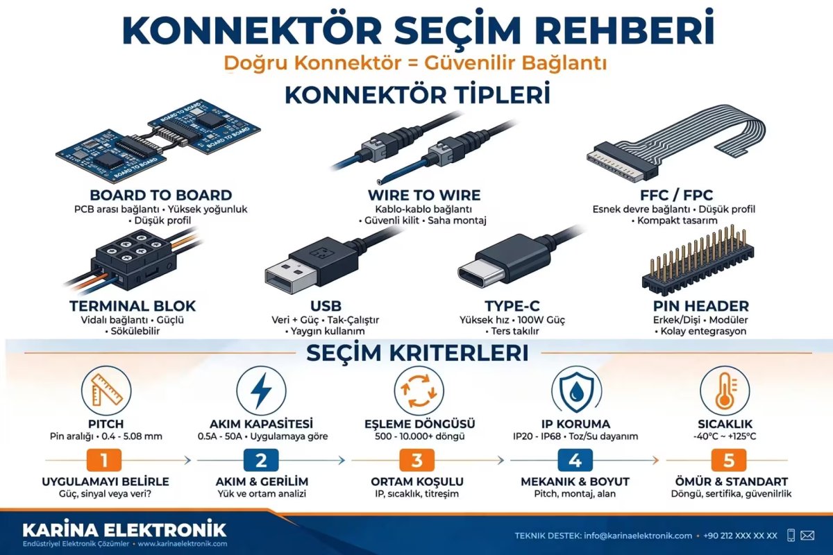
1. Connector Placement ErrorsOne of the most critical points. Wrong placement causes:Soldering difficulty and breakage under mechanical stressCable routing problems Increased EMI sensitivity
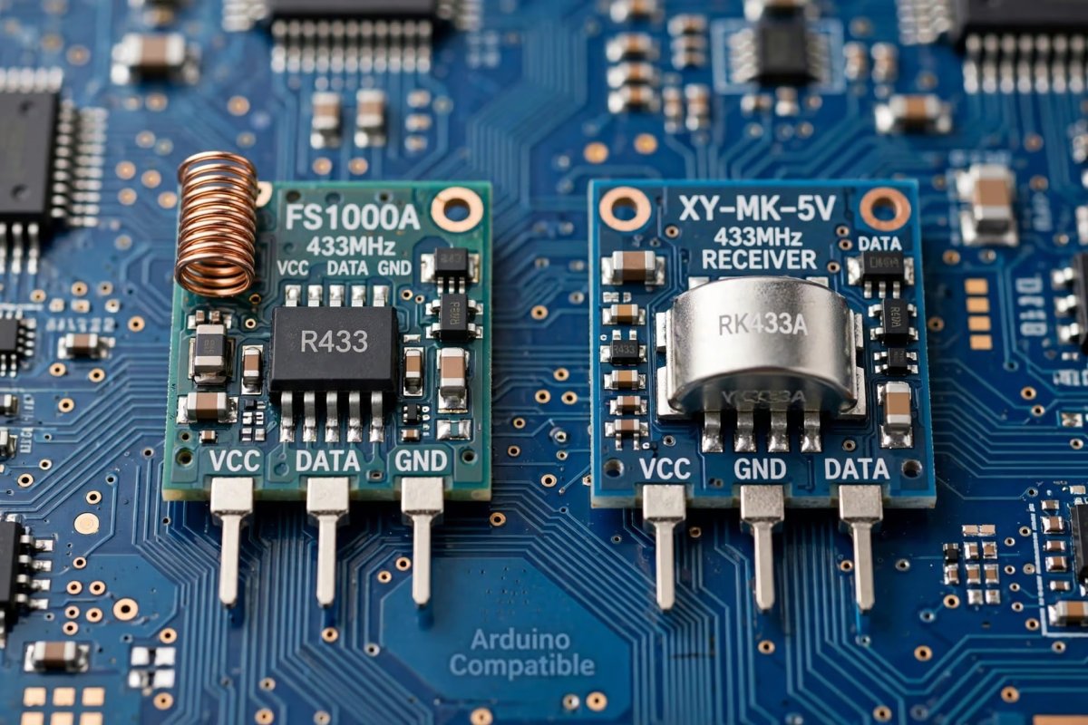
2. Pad and Footprint ErrorsWrong footprint -> component does not sit properly on PCB.Cold solderWeak electrical contact Assembly errors
3. EMI and Signal Integrity ProblemsIn high-frequency circuits:Data lossSignal distortion System instability Solution Methods - Checklist Use DFM checklistChoose correct footprint library (IPC-7351)Verify connector placement before productionDo EMI / EMC simulationApply prototype production testsConclusion
Even small mistakes in PCB design can turn into big problems in production. Design compliant with DFM principles both reduces cost and increases product reliability.
For professional PCB production and DFM analysis: https://www.karinaelektronik.com/